By: Karlyn Cynthia FM, Research Student at CCRI, Asia University, Taiwan
Abstract
The increasing growth of VLSI technology has influenced the development of complex integrated circuits which are used in modern systems. Although, the performance of these systems is initially analysed by the critical parameters which include: power consumption, propagation delay and area. They are frequently referred to as PPA which is power, performance and area. They do not depend on the architecture and involve certain trade-offs in the time of design process. This article will focus on the detailed analysis of particularly these three parameters, how their role impact on modern VLSI systems and optimization. Also, early research trends, as well as machine learning-based PPA prediction and analysis are spoken here to highlight the future trends in VLSI design.
Introduction
In the innovation of modern electronic systems like microprocessors, mobile devices and embedded systems, VLSI technology plays a vital role. Since the demand has been increasing for high-speed and energy-efficient devices, the people who are designing must be careful in enhancing the performance of the circuit, thereby maintaining low power consumption and reducing the area of the chip.
In any of the VLSI systems, power, delay and area are the primary parameters which will determine the efficiency of the circuit. The design making process is challenging as these parameters are highly equivalent and if improving one parameter usually leads to reduction of another. Handling these trade-offs has become more severe, as the integrated circuits remain to decrease.
Modern growth in design technologies, along with machine learning based techniques, continue to enhance the new predictions of these parameters which improves the design effectively and minimizing the evolution time.
Fundamentals of VLSI design: Power, Delay and Area
Power Consumption
One of the most demanding factors in VLSI design is power consumption, specifically for lightweight and battery-regulated devices. Power consumption consists of dynamic power and static power. Static power is also known as leakage power consumed in VLSI circuits and is obtained by currents leaking when the transistors are in OFF condition.
Dynamic power is obtained by the switching activity in CMOS circuits, whereas the leakage power becomes more prominent to power dissipation in nanoscale technology. The optimization of the circuit is necessary because as the complication increases, the power consumption also increases [3]. Power consumption in CMOS circuits consists of dynamic and static components, as illustrated in Fig. 1.
In order to decrease the consumption of power, different approaches like voltage scaling, transistor-level development and clock gating are used. To make the battery life enhanced and to reduce the formation of heat in early-stage devices, low-power design is needed [4].
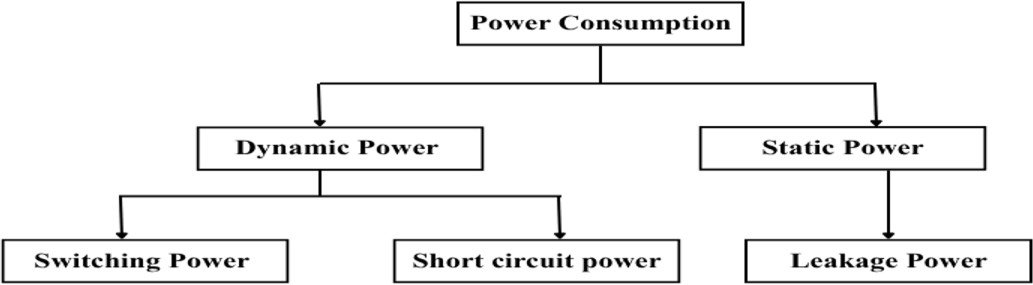
Figure 1: Components of power consumption in CMOS circuit
Delay
Delay usually indicates the time taken for a signal to pass through a circuit. The speed and the performance of the circuit is affected by the delay directly. In a circuit, the maximum delay known as the critical path delay which regulates the operating frequency.
In recent developments of VLSI circuits, due to the increase in the quantity of the circuit and rising effects, the interconnect delay has become a powerful factor. Techniques which reduce delay such as pipelining, parallel processing and logic restructuring are well developed [5].
Area
In VLSI, area serves as the physical silicon space employed by a circuit. Area is directly associated with the number of transistors and the design complexity. An elaborate comparison of power, delay, and area parameters is shown in Table 1.
In order to lower the fabrication costs and improving the chip density, reduction of area is necessary. Achieving an optimal balance is challenging, as reducing area may increase the delay or power consumption sometimes [1].
Performance Parameter | Definition | Impact on circuit | Optimization goal |
Power | Energy acquired by circuit | Affects battery life and heat | Minimize |
Delay | Time for the signal to propagate | Regulates speed | Minimize |
Area | Silicon space is needed | Affects cost and thickness | Minimize |
Table 1: Analysis of Power, delay and area performance
Trade-offs Between Power, Delay, and Area
The main threat in VLSI design is to maintain the trade-off among power, delay and area. Due to the type of design standards, these trade-offs are necessary.
Reduction in power consumption usually requires lowering the supply voltage, increasing the propagation delay. Thus, by adding the parallel structures or complicated architectures improves the speed which leads to improved area and power consumption.
Modern approaches have mostly focused on improving the power delay product, which contributes to a balanced range of performance and energy efficiency. When handling the common area constraints, powerful circuit designs minimize the power delay product (PDP) [6]. The trade-offs among power, delay, and area under different optimization goals are summarized in Table 2.
Also, by seeing that the layout-level effects at the time of the design stage, physically aware synthesis approaches have been created in order to improve both delay and power [7].
Optimization Focus | Effect on power | Effect on delay | Effect on area |
Minimize power | Power decreases | Delay increases | Area decreases |
Minimize delay | Power increases | Delay decreases | Area increases |
Minimize area | Area decreases | Delay increases | Power increases |
Table 2: Trade-offs among power, delay and area
Approaches for optimizing Power, performance and area
Power Optimization
Clock gating, power gating and dynamic voltage scaling comes under power optimization approaches. These approaches help in order to decrease the unwanted switching activity and static power which is nothing but leakage power.
In recent VLSI systems, dynamic voltage scaling is most commonly used. Based on the assignment conditions in order to gain energy efficiency, the supply voltage of the dynamic voltage scaling is modified [4].
Delay Optimization
By using the advanced architectural approaches like pipelining, parallelism and well-developed logic design, delay can be minimized.
Recent synthesis tools implement approaches such as gate downsizing, logic restricting and path optimization in order to gain timing closure and minimize the critical path delay [5].
Area Optimization
Without affecting the performance of the circuit or architecture significantly, area optimization targets on minimizing the hardware complexity. Area optimization helps in minimizing the transistor count for such approaches like approximate computing and efficient circuit logic designs. The trade-off relationship among power, delay, and area is depicted in Fig. 2.
Modern studies have presented that well improved and optimized arithmetic circuits can actually minimize the area where the circuit manages the sufficient performance levels [6].
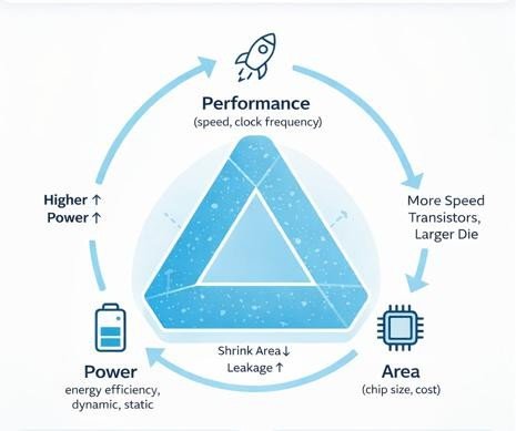
Figure 2: Trade-off relationship among Power, Delay, and Area in VLSI design
Growing Trends in PPA Optimization
Machine Learning based PPA prediction
In order to predict the power, delay and area in VLSI design, Machine Learning has newly been developed. This Machine Learning path minimizes the need for delayed simulations and makes the design process quicker.
A modern structure has identified high accuracy in prediction of PPA parameters straight from RTL designs, which implements the design analysis and optimization faster [2].
Smart Design Optimization
In order to automate design optimization by exploring huge number of datasets and looking on to the optimal design configurations, artificial intelligence approaches have mostly been used.
To attain better trade-offs among power, delay and area with minimized effort, these approaches help the designers to design the circuit efficiently.
Advanced Low-Power Design
The applications which are in the growing stage such as IoT and wearable devices need ultra- low power circuits. The advanced approaches that combine adaptive voltage scaling and energy efficient designs have been introduced to meet these particular needs [8].
Conclusion
In the definition of performance in VLSI systems, power, delay and area appears to be the primary parameters. Fulfilling the optimal balance among these parameters is a big threat in recent circuit designs.
This particular article has analysed the importance of PPA, the trade-offs which is present and different optimization approaches. By combining machine learning and AI based approaches, expecting future design techniques in VLSI to become more efficient which implements faster, smaller and energy-efficient electronic systems.
References
- T. Shan, “Advancements in VLSI low-power design: Strategies and optimization techniques,” 2024.
- A. Chattopadhyay and V. K. Sutrakar, “Machine Learning Framework for Early Power, Performance, and Area Estimation of RTL,” 2025.
- “Low power VLSI design research overview,” Academia.edu, 2024.
- “Low Power VLSI Design for Portable Devices,” IJESAT, 2025.
- “Timing optimization techniques in VLSI design,” 2025.
- “Recent trends in area and power-efficient arithmetic circuits,” IEEE VLSI, 2025.
- “Performance-driven optimization in VLSI physical design,” 2025.
- “Ultra-Low Power VLSI Design for Emerging Applications,” MDPI, 2024.
Cite As
Karlyn FM C, (2026) Power, Delay, and Area: The Core Trade-offs in Modern VLSI Design, Insights2Techinfo, pp.1